Material cycles in micro- and optoelectronics
Many of the materials used in microelectronic and optoelectronic devices are hardly promoted in the EU and have a limited occurrence worldwide. Furthermore, for some materials, it is currently not possible to easily scale the extraction. For example, while there are enormous gallium deposits, since extraction is typically coupled to that of zinc, gallium extraction cannot be considered individually.
In optoelectronics, there are also problems due to a shortage of materials; here, the rare element indium is of elemental importance. In every LED, indium is necessary to grow the light-generating layer. The wavelength of the emitted light can be adjusted via the indium content and there are currently no materials with which indium could be replaced. At the same time, the LED market is growing rapidly every year, especially due to the use of micro-LED arrays in modern displays. This leads to a shortage of indium and will result in a massive price increase of rare elements in the next years.
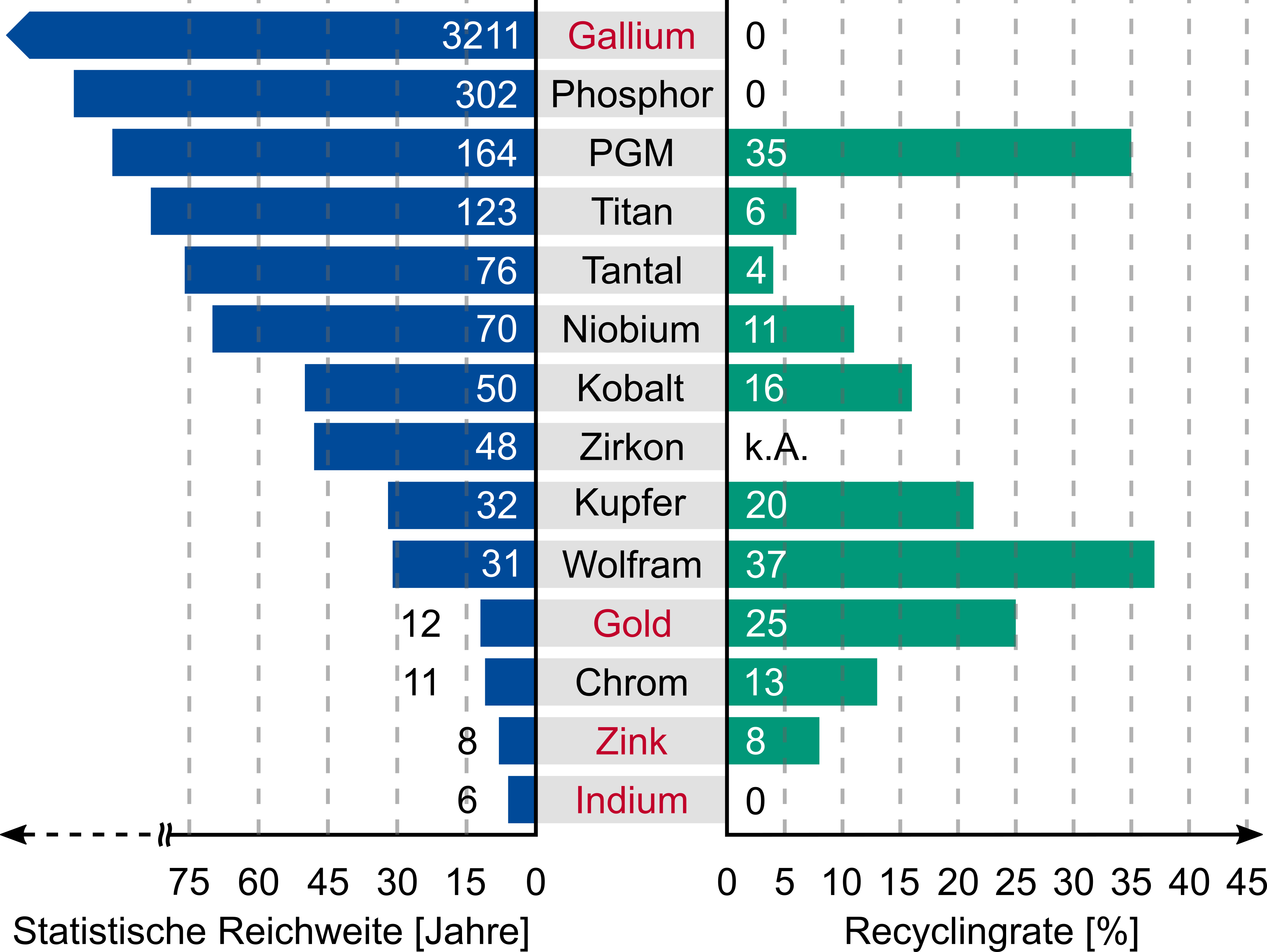
The statistical range indicates how long a material will be available with today's developed reserves and today's production. A CUTEC study entitled "Review and Update of Raw Material Parameters" summarizes the data of some important rare earths and has been regularly updated since then. This contrasts with a very low recycling rate of these materials.

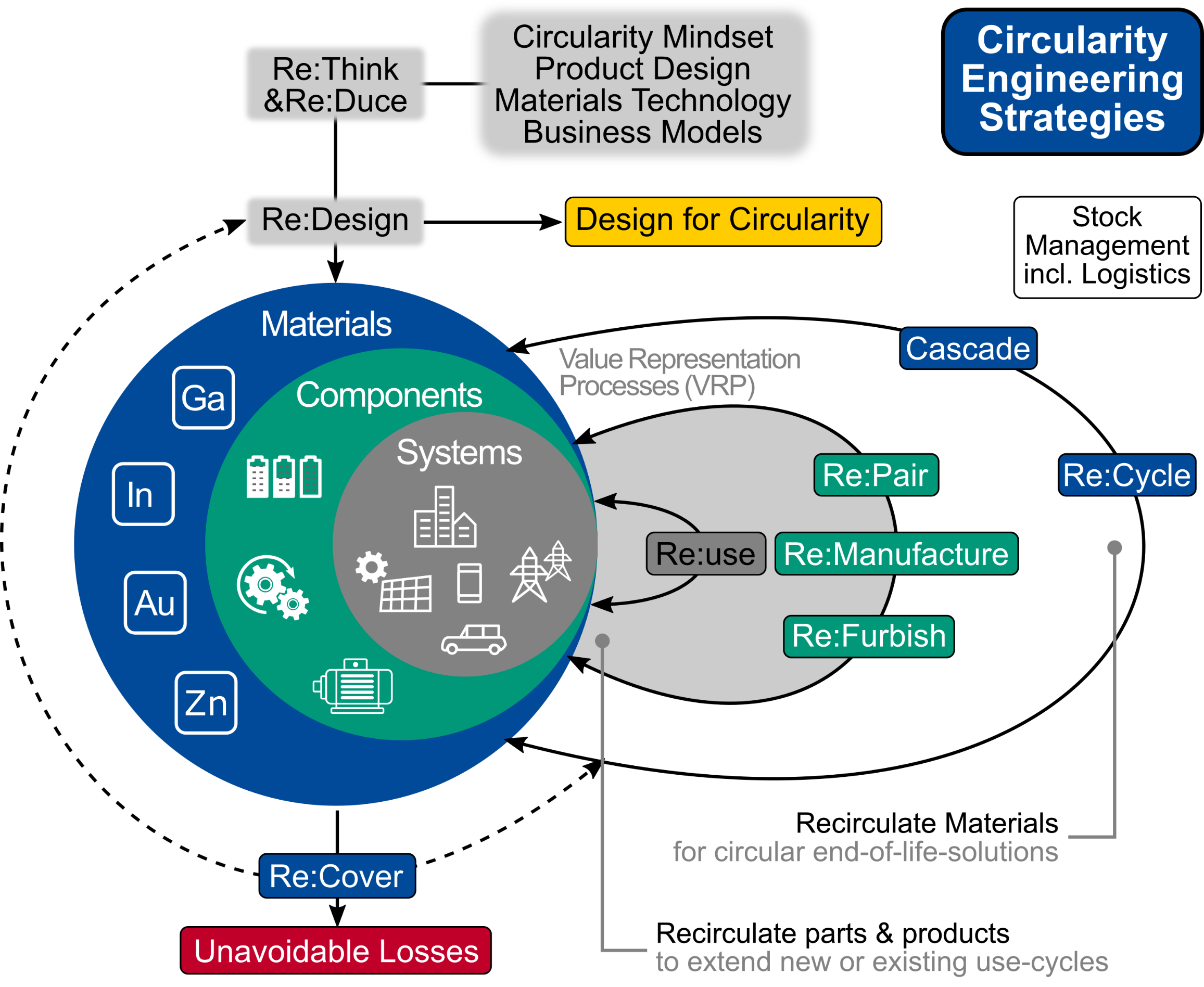
At INATECH, one of the research priorities is to develop materials and products in which the entire life cycle is considered and evaluated. The aim is to close the life cycle of components as completely as possible, so that sustainable availability is guaranteed. Within this "Circular Engineering" there are many partial aspects that have to be addressed in research. This includes above all the so-called Re's (Re-use, Re-pair, Re-cycle, Re-design).

The Gips-Schüle professorship for power electronics deals in one of its main research areas with the sublimation of compound semiconductors in order to develop concepts for the recycling of semiconductor devices. Furthermore, in cooperation with the other professorships of INATECH, strategies are developed to address the remaining re's and to establish concepts and methods for the sustainable availability of future devices.
Illustrated by the example of LEDs, concepts for the separation of the components (epitaxial semiconductor chip, package, converter and other electronic components) will be developed to evaluate the possibility of re-pair and re-manufacturing processes in a first step. In a second step, it should be possible to provide re-cycling processes so that rare raw materials can be recycled. With the knowledge gained from these research approaches, the third step is to derive design guidelines that will allow re-use in the future. In the case of LEDs, a design with simple separability of light-emitting diode and connection electronics would lead to significantly longer usability and simpler recycling options.

