Content
Widening the band gap of Cu(In,Ga)Se2 (CIGS) absorber layer has a big advantage not only for the single junction CIGS solar cells, but also for tandem devices where CIGS can be used as a top cell. This can be realized by either increasing the Ga content in the absorber layer to almost 100 at.% (In-free absorber layer) or by included Ag as a matrix element. Obtaining In-free absorber layer is of big relevance for obtaining green sustainable devices and materials, solving the problem of In-scarcity in nature.
However, the functional properties of the newly In-free absorber layer have to be further improved to meet the requirements for a high-performance solar cell. Hence, Re-Design of absorber layers with superior functional properties can be done through two directions that the CMC group is working on:
- Controlled growth by magnetron sputtering of absorbers layer with new functionalities.
- Nanocharacterization down to the atomic level using atom probe tomography and correlative microscopy.
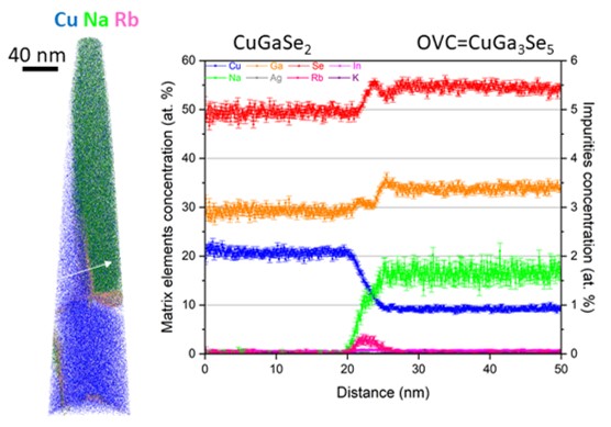
For example, below is an example of In-free CuGaSe2 (CGS) absorber layer investigated by atom probe tomography. The 3D reconstruction map given on the left provides the redistribution of Cu as a matrix element, but also of Na and Rb as light and heavy alkali. This study clearly reveals two important information:
- The formation of CuGa3Se5 OVC (ordered vacancy compound) inside the absorber layer;
- The redistribution of Na light alkali distinguishes neatly from that of the Rb heavy alkali: Na is mainly accumulated in the OVC compound, while Rb is found mainly accumulated at the interfaces.


